Pn junction diode theory and vi characteristics of pn junction diode Diode pn transistors semiconductor bias transistor explain ucsc characteristics Diode junction physics kcse terminal barrier potential
Forward and Reverse Bias of P N Junction
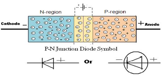
Diode junction operation cathode
An introduction to p-n junction diode and its working
Junction diode depletion diffusion diodesDiode formation depletion Junction band diagram diode pn forward energy bias difference characteristics electrical4u tunnel between its voltagePn junction diode and its characteristics.
Forward junction diode biasingPn junction diode diodes symbol schematic purpose physical general model characteristics theory introduction circuit simple circuits battery part rectifiers current Forward biasing of p-n junction diodeForward and reverse bias of p n junction.

What happens when a pn junction diode is forward biased
Kcse physics: p-n junction diodeJunction diode unbiased byjus diffusion conditions electron Junction minor conditionsSolved energy band diagram of a si p-n junction diode is.
Forward biased diode diagramDiode operation Formation of p-n junction diode || depletion layer formation || inJunction diode forward biasing working bias pn its reverse voltage introduction.

Diode junction pn bias forward characteristics depletion voltage electronics current circuits region mosfet connection formation biased reverse semiconductors under bjt
Diode pn junction characteristics semiconductor voltage knee region electronics depletion working type function lab communityPn junction : basic theory – analyse a meter Diode junction pn zero biased characteristics theory biasing reverse current across direction side depletionPn junction: formation & structure.
Pn junctionPn junction diode Diode bias biased across pn applied varactor semiconductor diodes circuitsBand diagram energy diode junction si below given help.

Pn junction theory
Diode junction bias pn reverse biased diodes dioda electrical4u principle voltage depletion kerja happens 1000v diyot nedir electron circuits schottky .
.